

EasyEDA is a Online PCB design and Simulation Tool. We have already covered this tool in detail in this article EasyEDA for Electronic Circuit Design. Today, we will learn ‘How to use EasyEDA’ by designing and simulating the Simple 100 watt Inverter Circuit, with the help of Easy EDA. We have also covered the working and demonstration of this circuit here: 12V DC to 220V AC Inverter Circuit
Before going further let’s talk a bit about EasyEDA, its Online Software used to Design Schematics for circuits and to Simulate them and also to Design PCB Layout for the same. It’s basically a tool that is used to design projects. As told its online software, so one need not to download any application for this, you can simple Sign Up or Login to the website and play along, as you please. As its online tool, that makes its platform independent and can be run on any OS (Windows/Linux/Mac) and Browser (Internet Explorer/ Firefox/ Chrome/ Safari).
As no software is being downloaded, no need to be afraid of malware and virus. Once a project is designed, we need not to worry about misplacing it because it will be stored at EasyEDA website. So we can access the file anytime. With many features being added day by day, the EasyEDA website can be depicted as a promising tool for Electronic Hobbyist and Engineers.
Getting Started with EasyEDA:
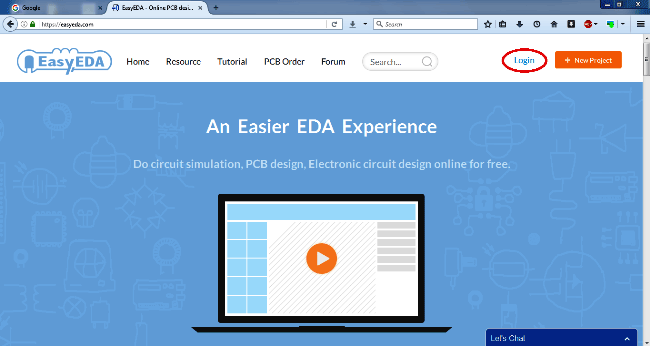
First to design the circuit we need to go to EasyEDA website: https://easyeda.com. The website is shown in the figure.
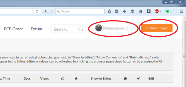
Then hit on LOGIN button to create an account. You can create a new Account on EasyEDA or you can Login with your Google or QQ account. Here we are Login with Google Account:

Login with your Gmail details (assuming you already have a Gmail account), and you will see your name on upper right corner.
Drawing the Schematic using EasyEDA:
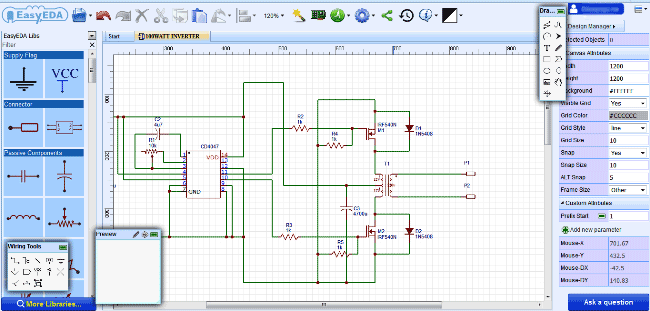
After creating the account, click on New Project as shown in above figure to start drawing a new schematic. Once you enter the drawing board pick up all the components that are needed from the libraries. If you cannot find the component, click on MORE LIBRARIES option and then search for your component, as shown below.

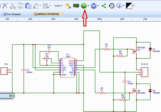
Pick all the components from the left panel and draw the schematic as shown in below figure. Click on the desired component to select and again click on the canvas to Drop that component. Right click or Esc button to exit after placing component. Wiring can be simply done by dragging the wire between end points of components, like we do in most of the Circuit drawing softwares like Proteus. Also to change the properties or attributes of any components, just click on that component, and change the attributes from the Right side panel.
Short keys can be found and edited in the Blue gear button at the Top. You can try some ‘hand on’ by playing with these examples: EasyEDA examples
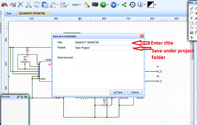
After the drawing is completed, Save the schematic under your project name so that you can do the simulation.
Simulating the Circuit in EasyEDA:
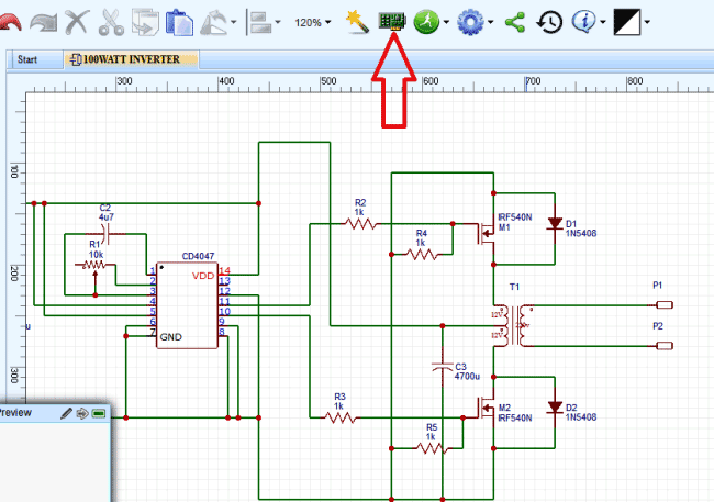
After saving the circuit, click on “Green Button” on top of screen for Simulation and choose “Run the document”.
After that you have to configure the simulation you want to run. As shown in below figure, you have five type of simulation.

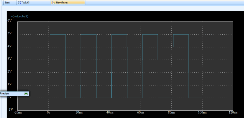
For now we will stick with transient, as told before we are designing inverter circuit here, the AC output provided by the inverter is to drive home appliances. For that to happen, the inverter circuit should be operated at 50Hz frequency as it is the AC line frequency. We will choose the appropriate START and STOP TIME for the simulation graph to be understandable.
Once the simulation completes you can see the graph at the chosen terminal. The terminal should be chosen by bringing the probe to that point. You can select the probe as shown below; drag it to the point where you want to see the graph.

On simulation you will have a graph as shown below. These waveforms can be saved and exported in different formats like JPG, PDF, PNG etc.
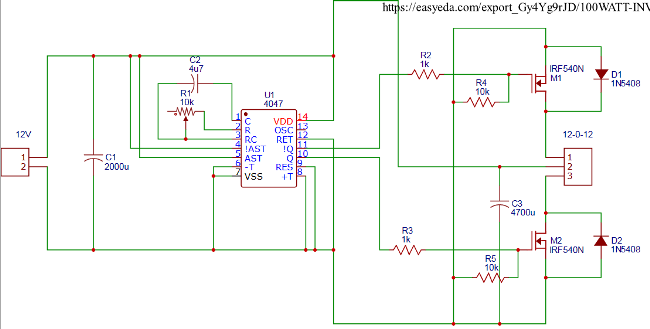
The exported figure shows the Circuit Diagram of 100 watt Inverter using Easy EDA,
Check its full working here: 12V DC to 220V AC Inverter Circuit
PCB layout conversion using EasyEDA:
After we go to schematic board, click on the “PROJECT TO PCB” option as shown in below figure. Once you click on that you will enter to PCB design board. In case if there are any components on the schematic which don’t have PCB traces, you will be asked to choose the most appropriate one to proceed. Choose the appropriate one based on your view and submit it.
After entering the PCB design, all the components will be distributed around the PCB model board as shown below.
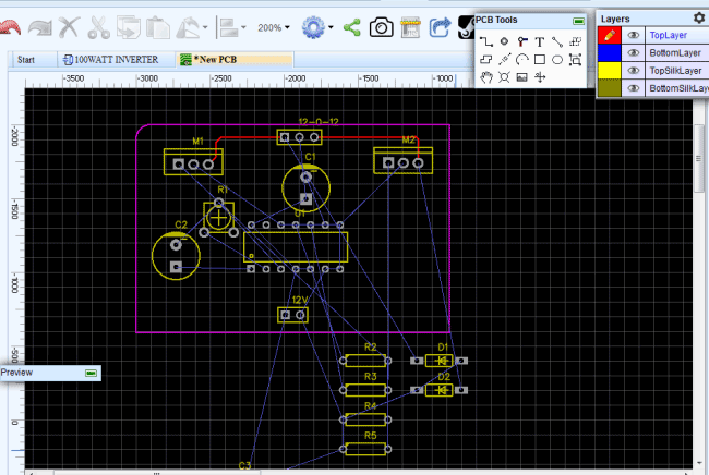
Arrange all the components in the orderly fashion as we arrange the books in a shelf. Once everything is arranged you should be having input at one end and output on the other, as shown below.

Now trace the light blue lines on the board without intercepting one another, you can do as many loops as you want. These traces must not be too close to one another.
Once the tracing is completed you will have something as below,

After that choose PRINT in the FILE menu, to get the PCB board trace. Print the appropriate layer by selecting the option, since we are using a single layer, we can leave the configuration as it is.

Once you print it you will have a document as,

You can print the picture on to glossy paper for PCB etching or you can give the module to PCB manufacturers for mass production.
With this we have concluded the 100watt inverter design using EasyEDA.
Easyeda seems to be a ray of hope for many electronic circuit developers, through this mean building any systematic gadget or software will be easier & thorough enough. We are all waiting for a more enhanced online mechanism to deal with the failures.
are the two diodes are forward biased or reverse biased in 100watt inverter. using 4047 ic
Hi Sir,
Could you please tell me how to calculate the C1 capacitor microfarad value for DC AC inverter like you have given 2000uf to C1 for 100W please?
Hi, sir
can you sent my mail this diagram and code
Thank you

Easyeda seems to be a ray of hope for many electronic circuit developers, through this mean building any systematic gadget or software will be easier & thorough enough. We are all waiting for a more enhanced online mechanism to deal with the failures.