
 Transistor")
IGBT is a short form of Insulated Gate Bipolar Transistor, combination of Bipolar Junction Transistor (BJT) and Metal oxide Field effect transistor (MOS-FET). It’s is a semiconductor device used for switching related applications.
As IGBT is a combination of MOSFET and Transistor, it has advantages of the both transistors and MOSFET. MOSFET has advantages of high switching speed with high impedance and on the other side BJT has advantage of high gain and low saturation voltage, both are present in IGBT transistor. IGBT is a voltage controlled semiconductor which enables large collector emitter currents with almost zero gate current drive.
As discussed, IGBT has the advantages of both MOSFET and BJTs, IGBT has insulated gate same as like typical MOSFETs and same output transfer characteristics. Although, BJT is current controlled device but for the IGBT, the control depends on the MOSFET, thus it is voltage controlled device, equivalent to the standard MOSFETs.
IGBT Equivalent Circuit and Symbol
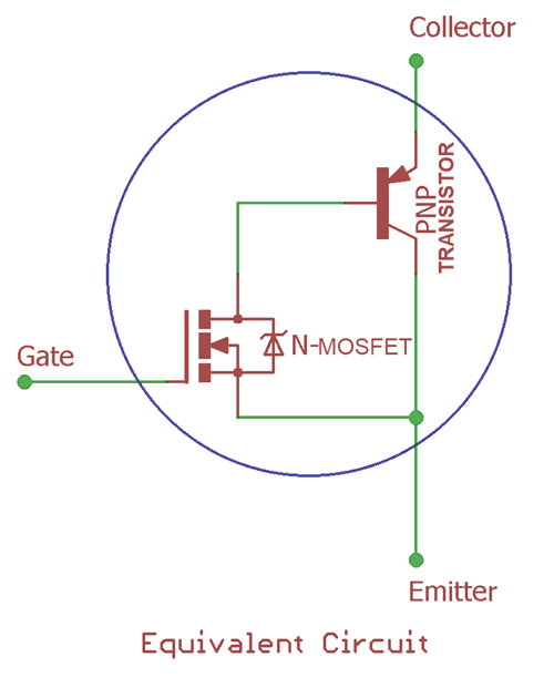
In the above image the equivalent circuit of IGBT is shown. It’s same circuit structure used in Darlington Transistor where two transistors are connected exactly the same way. As we can see the above image, IGBT combines two devices, N channel MOSFET and PNP transistor. N channel MOSFET is driving the PNP transistor. A standard BJT’s pin out includes Collector, Emitter, Base and a standard MOSFET pin out includes Gate, Drain and Source. But in the case of IGBT transistor Pins, it is the Gate, which is coming from the N-channel MOSFET and the Collector and Emitter are coming from the PNP transistor.
In the PNP transistor, collector and Emitter is conduction path and when the IGBT is switched on it is conducted and carry the current through it. This path is controlled by the N channel MOSFET.
In case of the BJT, we calculate the gain which is denoted as Beta ( ), by dividing the output current by the input current.
β = Output Current / Input Current
But, as we know, MOSFET is not a current controlled device; it is a voltage controlled device, there is no input current across the MOSFET’s gate. So, the same formula which is applied for calculating the gain of BJT’s, is not applicable for the MOSFET technology. The MOSFET’s gate is isolated from the current conductions path. MOSFET’s gate voltage changed the output current conduction. Thus the gain is the ratio of output voltage changes with the input voltage changes. This is true for the IGBT. An IGBT’s gain is the ratio of output current changes with the input gate voltage changes.
Due to high current capabilities, the BJT’s high current is controlled by the MOSFET gate voltage.
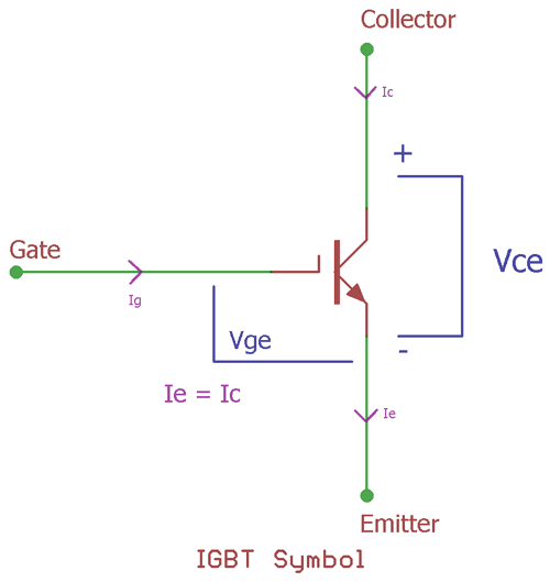
In the above image, symbol of IGBT is shown. As we can see, the symbol includes Transistor’s collector emitter portion and the MOSFET’s gate portion. The three terminals are shown as Gate, collector and Emitter.
When in conducting or switched ‘ON’ mode the current flow from collector to emitter. Same thing happens for the BJT transistor. But in the case of IGBT there is Gate instead of base. The difference between Gate to Emitter voltage is called as Vge and the voltage difference between collector to emitter is called as Vce.
The emitter current (Ie) is almost same as the collector current (Ic), Ie = Ic. As the current flow is relatively same in both collector and emitter, the Vce is very low.
Learn more about BJT and MOSFET here.
Applications of IGBT:
IGBT is mainly used in Power related applications. Standard power BJT’s have very slow response properties whereas MOSFET is suitable for fast switching application, but MOSFET is a costly choice where higher current rating is required. IGBT is suitable for replacing power BJTs and Power MOSFETs.
Also, IGBT offers lower ‘ON’ resistance compared with BJTs and due to this property the IGBT is thermal efficient in high power related application.
IGBT applications are vast in electronics field. Due to low on resistance, Very high current rating, high switching speed, zero gate drive, IGBTs are used in High power motor control, Inverters, switched mode power supply with high frequency converting areas.
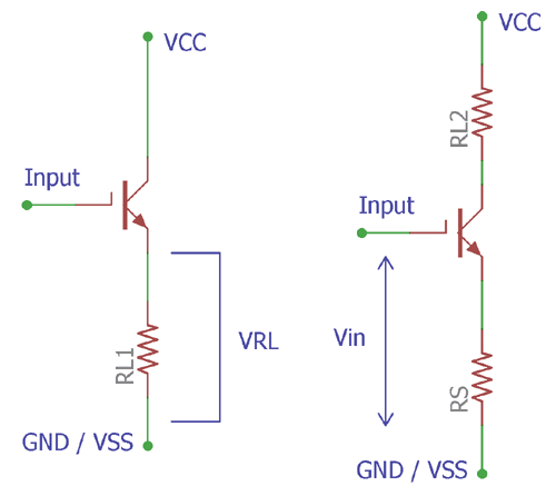
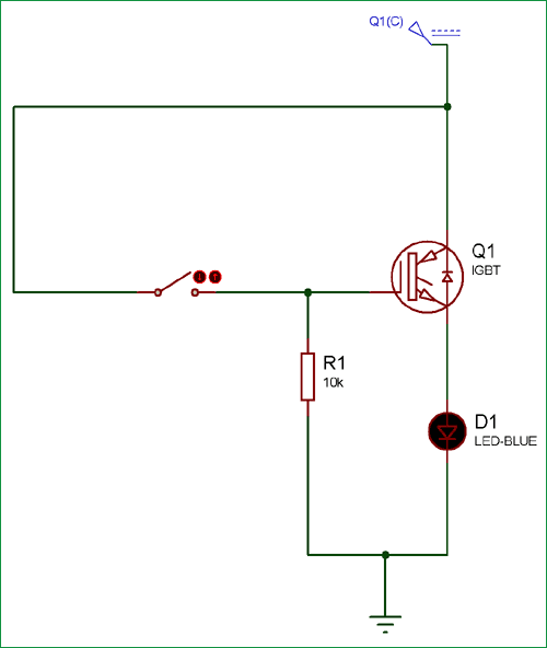
In the above image, basic switching application is shown using IGBT. The RL, is a resistive load connected across IGBT’s emitter to ground. The voltage difference across the load is denoted as VRL. The load can be inductive also. And on the right side a different circuit is shown. The load is connected across collector where as a current protection Resistor is connected across the emitter. The current will flow from collector to emitter in both cases.
In case of BJT’s we need to supply constant current across the base of the BJT. But in case of the IGBT, same as like MOSFET we need to provide constant voltage across the gate and the saturation is maintained in constant state.
On the left case, the voltage difference, VIN which is the potential difference of the Input (gate) with the Ground / VSS, controls the output current flowing from the collector to emitter. The voltage difference between VCC and GND is almost same across the load.
On the right side circuit, the current flowing through the load is depends on the voltage divided by the RS value.
IRL2 = VIN / RS
The Insulated Gate Bipolar Transistor (IGBT) can be switched ‘ON’ and ‘OFF’ by activating the gate. If we make the gate more positive by applying voltage across the gate, the IGBT’s emitter keeps the IGBT in its “ON“state and if we make the gate negative or zero push the IGBT will remain in “OFF” state. It is same as like BJT and MOSFET switching.
IGBT I-V Curve and Transfer Characteristics
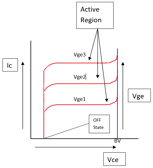
In the above image, I-V characteristics are shown depending on the different gate voltage or Vge. The X axis denotes collector emitter voltage or Vce and the Y axis denotes the collector current. During the off state the current flowing through the collector and the gate voltage is zero. When we change the Vge or the gate voltage the device goes in to the active region. Stable and continuous voltage across gate provides continuous and stable current flow through the collector. Increase of Vge is proportionally increasing the collector current, Vge3 > Vge2 > Vge3. BV is the breakdown voltage of the IGBT.
This curve is almost identical with BJT’s I-V transfer curve, but here Vge is shown because IGBT is a voltage controlled device.
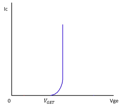
In the above image, the Transfer characteristic of IGBT is shown. It is almost identical with PMOSFET. The IGBT will go to the “ON” state after Vge is greater than a threshold value depending on the IGBT specification.
Here is a comparison table which will give us a fair picture about the difference between IGBT with POWER BJT’s and Power MOSFETs.
|
Device Characteristics |
IGBT |
Power MOSFET |
POWER BJT |
|
Voltage Rating |
More than 1kV (Very High) |
Less than 1kV (High) |
Less than 1kV (High) |
|
Current Rating |
More than 500A (High) |
Less than 200A (High) |
Less than 500A (High) |
|
Input Device |
Voltage, Vge, 4-8V |
Voltage, Vgs, 3-10V |
Current, hfe, 20-200 |
|
Input Impedance |
High |
High |
Low |
|
Output Impedance |
Low |
Medium |
Low |
|
Switching Speed |
Medium |
Fast (nS) |
Slow (uS) |
|
Cost |
HIgh |
Medium |
Low |
In the next video, we will see the switching circuit of IGBT transistor.

What is the valuu of IGBT to ON for Vge=4v~5V and output Vce=250V and above , & Ic=Ie=3A and above and working time below 10 ms.