

In previous tutorial of half adder circuit construction, we had seen how computer uses single bit binary numbers 0 and 1 for addition and create SUM and Carry out. Today we will learn about the construction of Full-Adder Circuit.
Here is a brief idea about Binary adders. Mainly there are two types of Adder: Half Adder and Full Adder. In half adder we can add 2-bit binary numbers but we cant add carry bit in half adder along with the two binary numbers. But in Full Adder Circuit we can add carry in bit along with the two binary numbers. We can also add multiple bits binary numbers by cascading the full adder circuits which we will see later in this tutorial. We also use IC 74LS283N to practically demonstrate the Full Adder circuit.
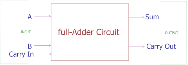
Full Adder Circuit:
So we know that Half-adder circuit has a major drawback that we do not have the scope to provide ‘Carry in’ bit for addition. In case full adder construction, we can actually make a carry in input in the circuitry and could add it with other two inputs A and B. So, in the case of Full Adder Circuit we have three inputs A, B and Carry In and we will get final output SUM and Carry out. So, A + B + CARRY IN = SUM and CARRY OUT.
As per mathematics, if we add two half numbers we would get full number, same thing is happening here in full adder circuit construction. We add two half adder circuits with an extra addition of OR gate and get a complete full adder circuit.
Full Adder Circuit Construction:
Let’s see the block diagram,
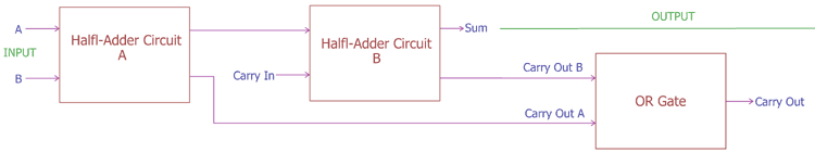
Full adder circuit construction is shown in the above block diagram, where two half adder circuits added together with a OR gate. The first half adder circuit is on the left side, we give two single bit binary inputs A and B. As seen in the previous half adder tutorial, it will produce two outputs, SUM and Carry out. First half adder circuit’s SUM output is further provided to the second half adder circuit’s input. We provided the carry in bit across the other input of second half order circuit. Again it will provide SUM out and Carry out bit. This SUM output is the final output of the Full adder circuit. On the other hand the Carry out of First half adder circuit and the Carry out of second adder circuit is further provided into OR logic gate. After logic OR of two Carry output, we get the final carry out of full adder circuit.
The Final Carry out represents the most significant bit or MSB.
If we see the actual circuit inside the full adder, we will see two Half adders using XOR gate and AND gate with an additional OR gate.
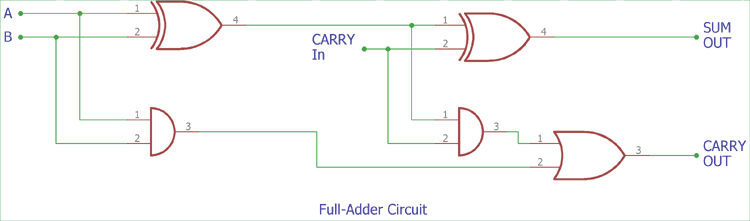
In the above image, instead of block diagram, actual symbols are shown. In previous half-adder tutorial, we had seen the truth table of two logic gates which has two input options, XOR and AND gates. Here an extra gate is added in the circuitry, OR gate.
You can learn more about Logic gates here.
Truth Table of Full Adder Circuit:
As Full adder circuit deal with three inputs, the Truth table also updated with three input columns and two output columns.
|
Carry In |
Input A |
Input B |
SUM |
Carry Out |
|
0 |
0 |
0 |
0 |
0 |
|
0 |
1 |
0 |
1 |
0 |
|
0 |
0 |
1 |
1 |
0 |
|
0 |
1 |
1 |
0 |
1 |
|
1 |
0 |
0 |
1 |
0 |
|
1 |
1 |
0 |
0 |
1 |
|
1 |
0 |
1 |
0 |
1 |
|
1 |
1 |
1 |
1 |
1 |
We can also express the full adder circuit construction in Boolean expression.
For the case of SUM, We first XOR the A and B input then we again XOR the output with Carry in. So, the Sum is (A XOR B) XOR C.
We can also express it with (A ⊕ B) ⊕ Carry in.
Now, for the Carry out, it is A AND B OR Carry in (A XOR B), which is further represented by A.B + (A ⊕ B).
Cascading Adder Circuits
As of now, we described the construction of single bit adder circuit with logic gates. But what if we want to add two more than one bit numbers?
Here is the advantage of full adder circuit. We can cascade single bit full adder circuits and could add two multiple bit binary numbers. This type of cascaded full adder circuit is called as Ripple Carry Adder circuit.
In case of Ripple Carry Adder circuit, Carry out of the each full adder is the Carry in of the next most significant adder circuit. As the Carry bit is ripple into the next stage, it is called as Ripple Carry Adder circuit. Carry bit is rippled from the left to right (LSB to MSB).
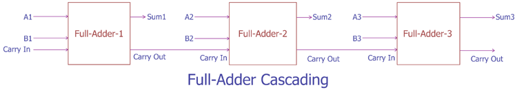
In the above block diagram we are adding two three bit binary numbers. We can see three full adder circuits are cascaded together. Those three full adder circuits produce the final SUM result, which is produced by those three sum outputs from three separate half adder circuits. The Carry out is directly connected to the next significant adder circuit. After the final adder circuit, Carry out provide the final carry out bit.
This type of circuit also has limitations. It will produce unwanted delay when we try to add large numbers. This delay is called as Propagation delay. During the addition of two 32 bit or 64 bit numbers, the Carry out bit which is the final output’s MSB, wait for the changes in previous logic gates.
To overcome this situation, very high clock speed is required. However, this problem can be solved using carry look ahead binary adder circuit where a parallel adder is used to produce carry in bit from the A and B input.
Practical Demonstration of Full Adder Circuit:
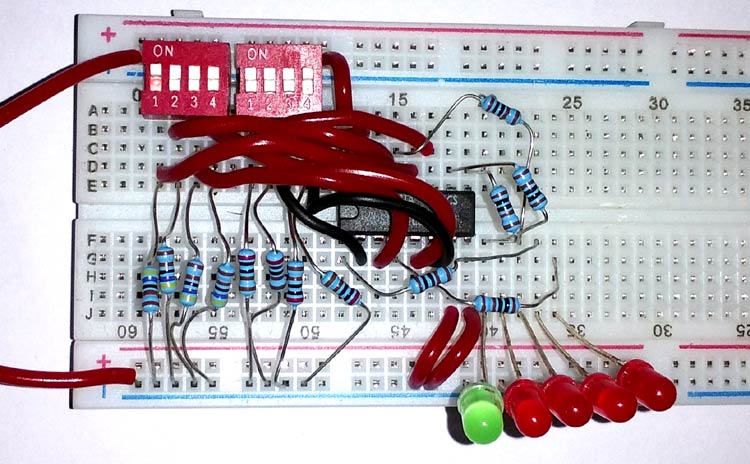
We will use a full adder logic chip and add 4 bit binary numbers using it. We will use TTL 4 bit binary adder circuit using IC 74LS283N.
Components used-
- 4pin dip switches 2 pcs
- 4pcs Red LEDs
- 1pc Green LED
- 8pcs 4.7k resistors
- 74LS283N
- 5 pcs 1k resistors
- Breadboard
- Connecting wires
- 5V adapter
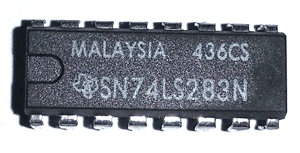
In the above image 74LS283N is shown.74LS283N is a 4bit full adder TTL chip with carry look ahead feature. The pin diagram is shown in the schematic below.

Pin 16 and Pin 8 is VCC and Ground respectively, Pin 5, 3, 14 and 12 are the first 4 bit number (P) where the Pin 5 is the MSB and pin 12 is the LSB. On the other hand, Pin 6, 2, 15, 11 are the second 4 bit number where the Pin 6 is the MSB and pin 11 is the LSB. Pin 4, 1, 13 and 10 are the SUM output. Pin 4 is the MSB and pin 10 is the LSB when there are no carry out.
4.7k resistors are used in all input pin to provide logic 0 when the DIP switch is in OFF state. Due to the resistor, we can switch from logic 1 (binary bit 1) to logic 0 (binary bit 0) easily. We are using 5V power supply. When the DIP switches are ON, the input pins get shorted with 5V; we used red LEDs to represent the SUM bits and green Led for Carry out bit.
Also check the Demonstration Video below where we have shown adding two 4-bit binary Numbers.
