

In this tutorial, we will learn about Wein Bridge Oscillator which was developed by a German physicist Max Wien. It is originally developed for calculating the capacitance where the resistance and the frequency are known. Before going to the further in depth discussion about what actually the Wein Bridge Oscillator and how it is used, let’s see what is Oscillator and what Wein Bridge Oscillator is.
Wein Bridge Oscillator:
As in the previous tutorial of RC Oscillator, A resistor and capacitor is required to produce a phase shift, and If we connect an amplifier in inverting spec and connect the amplifier and RC networks with a feedback connection the output of the amplifier start to produce a sinusoidal waveform by oscillation.
In a Wien bridge oscillator two RC networks are used across an amplifier and produce an oscillator circuit.
But why should we choose Wien bridge oscillator?
Because of the following points the Wien bridge oscillator is a wiser choice for producing Sinusoidal wave.
- It is stable.
- The distortion or the THD (Total Harmonic Distortion) is under controllable limit.
- We can change the frequency very effectively.
As told before that Wein Bridge oscillator has two stage RC networks. That means it consists two non-polar capacitors and two resistors in a High pass and Low pass filter formation. One resistor and one capacitor in series on the other hand one capacitor and one resistor in parallel formation. If we construct the circuit the schematic will be just look like this one:-
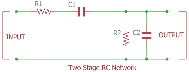
As clearly seen there are two capacitors and two resistors are used. Both RC stage which act as High Pass and Low pass filter connected together which is the product of a Band pass filter which accumulate the frequency dependency of two order stages. The R1 and R2 Resistance are same and also the C1 and C2 capacitance is same.
Wein Bridge Oscillator Output Gain and Phase Shift:
What happens inside the RC network circuit in the above image is very interesting.
When Low frequency is applied the first capacitor (C1) reactance is high enough and block the input signal and resist the circuit to produce 0 output, on the other hand, Same thing happen in a different way for the second capacitor (C2) which is connected in parallel condition. C2 reactance is become too low and bypass the signal and again produce 0 outputs.
But in case of a medium frequency when the C1 reactance is not high and the C2 is reactance is not low it will give output across the C2 point. This frequency referred as Resonant Frequency.
If we see in depth inside the circuitry we will see that the reactance of the circuit and the Resistance of the circuit is equal if the resonant frequency is achieved.
So, there are two rules applied in such case when the circuit is provided by the resonant frequency across the Input.
A.The Phase difference of Input and output is equal to 0 degree.
B.As it is in 0 degree the output will be maximum. But how Much? It is closely or accurately 1/3rd of the input signal’s magnitude.
If we see the output of the circuitry we will understand those points.

The output is exactly as the same curve as the image showing. At Low Frequency from 1Hz the output is less or almost 0 and increasing with the frequency at input upto the resonant frequency, and when the resonant frequency is reached the output is at its maximum peak point and continuously decreasing with the increasing of the frequency and again it’s produce 0 output at high frequency. So it is clearly passing a certain frequency range and producing the output. That’s why previously it was described as frequency dependable variable Band (Frequency Band) pass filter. If we closely look at the phase shift of the output we will clearly see the 0 degree phase margin across the output at the proper resonant frequency.

In this Phase output curve the phase is exactly 0 degree at the Resonance frequency and it is started from 90 degree to decreasing at 0 degree when input frequency increased until resonance frequency is achieved and after that the phase continue to decrease at the end point of -90 degree. There are two terms are used in both case, If the phase is positive it is called as Phase Advance and in case of negative it is called as Phase Delay.
We will see the output of the filter stage in this simulation video:
In this video 4.7k used as R in both R1 R2 and the 10nF capacitor is used for both C1 and C2. We applied sinusoidal wave across the stages and in the oscilloscope Yellow Channel is showing the input of the circuitry and the blue line is showing output of the circuitry. If we look closely the output amplitude is 1/3rd of the input signal and the output phase is almost identical as 0 degree phase shift in resonant frequency as discussed before.
Resonance Frequency and Voltage Output:
If we consider that R1 = R2 = R or the same resistor is used, and for the selection of the capacitor C1 = C2 = C the same capacitance value is used then the resonance frequency will be
Fhz = 1 / 2πRC
The R stands for Resistor and the C stands for the capacitor or capacitance, and the Fhz if Resonance frequency.
If we want to calculate the Vout of the RC network we should see the circuit in a different way.
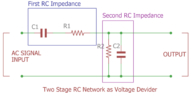
This RC network work with AC signals Input. Calculating circuitry resistance in case of AC rather than calculating circuitry resistance in case of DC is a bit tricky.
RC network creates impedance which acts as resistance on an applied AC signal. A voltage divider has two resistances, in these RC stages the two resistances is First filter (C1 R1) impedance and the Second filter (R2 C2) impedance.
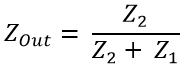
As there are a capacitor is connected either series or in parallel configuration then the Impedance formula will be:-
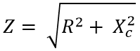
Z is the symbol of Impedance, R is the Resistance and the Xc stands for the capacitive reactance of the capacitor.
By using the same formula we can calculate the first stage impedance.
In case of the second stage, the formula is same as calculating the parallel equivalent resistor,
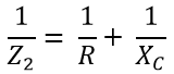
Z is the impedance,
R is the Resistance,
X is the Capacitor
The Final Impedance of the circuitry can be calculated using this formula:-
We can calculate a Practical Example and see the Output In such case.
If we calculate the value and see the result we will see that the output voltage will be 1/3rd of the input voltage.
If we connect the two stage RC filter output into a non-inverting amplifier input pin or +Vin pin, and adjust the gain to recover the loss the output will produce a sinusoidal wave. That is Wien bridge oscillation and the circuitry is Wein Bridge Oscillator circuit.
Working and Construction of Wein Bridge Oscillator:
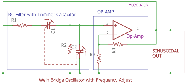
In the above image, the RC filter is connected across an op-amp which is in a non-inverting configuration. R1 and R2 is Fixed value resistor whereas the C1 and C2 is a variable trim capacitor. By varying the value of those two capacitors at the same time we could get proper oscillation from a lower range to upper range. It’s very useful if we want to use the Wein bridge oscillator to produce sinusoidal wave at different frequency from a lower to upper range. And the R3 and R4 are used for the op-amp feedback gain. The output gain or the amplification is highly dependable on those two value combinations. As the two RC stages drop the output voltage at 1/3rd it is essential to recover that back. It is also a wiser choice to get at least 3x or more than 3x (4x preferred) gain.
We can calculate the gain using 1+ (R4/R3) relation.
If we again see the image we can see that the feedback path of the operational amplifier from the output is directly connected to the RC filter input stage. As the two stage RC filter has a property of 0 degree phase shift in the resonance frequency region, and directly connected to the op-amp positive feedback let’s assume it is xV+ and the in the negative feedback the same voltage is applied which is xV- with the same 0 degree Phase the op-amp differentiate the two input and rule out the negative feedback signal and due to that continues as the output connected across RC stages the op-amp start to oscillate.
If we use a higher slew rate, higher frequency op-amp the output frequency can be maximized by a wide amount.
Few High frequency op-amps are in this segment
Also we need to remember as in previous RC oscillator tutorial we discussed about the loading effect, we should choose the op-amp with high input impedance more than the RC filter to reduce loading effect and ensure proper stable oscillation.
- LM318A
- LT1192
- MAX477
- LT1226
- OPA838
- THS3491 which is 900 mHz High seed op-amp!
- LTC6409 which is 10 Ghz GBW Differential op-amp. Not to mention this requires special add on circuitry and exceptionally good RF design tactics to achieve this High Frequency output as well.
- LTC160
- OPA365
- TSH22 Industrial grade op-amp.
Practical Example of Wein Bridge Oscillator:
Let’s calculate a practical example value by choosing the Resistor and capacitor value.
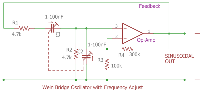
In this image, for the RC oscillator a 4.7k resistor is used for both R1 and R2. And a trimmer capacitor used which has two poles contains 1-100nF for C1 and C2 trimming capacity. Lets calculate the Frequency of oscillation for 1nF, 50nF and 100nF. Also we will calculate the gain of the op-amp as R3 selected as 100k, and R4 selected as 300k.
As calculating the frequency is easy by the formula of
Fhz = 1 / 2πRC
For the value of C is 1nF and for the resistor is 4.7k the Frequency Will be
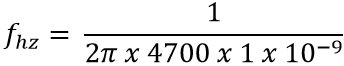
Fhz = 33,849 Hz or 33.85 KHz
For the value of C is 50nF and for the resistor is 4.7k the Frequency Will be
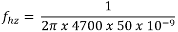
Fhz = 677Hz
For the value of C is 100nF and for the resistor is 4.7k the Frequency Will be
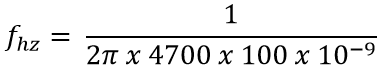
Fhz = 339Hz
So the Highest Frequency we can achieve using 1nF which is 33.85 Khz and the lowest frequency we can achieve using 100nF is 339Hz.
The gain of the op-amp is 1+(R4/R3)
R4 = 300k
R3 = 100k
So the Gain = 1+(300k+100k) = 4x
The op-amp will produce 4x gain of the input across the non-inverted “positive” pin.
So by using this way we can produce variable frequency bandwidth Wein Bridge Oscillator.
Applications:
Wein Bridge Oscillator used in wide level of applications in the field of electronics, from finding the exact value of the capacitor, For generating 0 degree phase stable oscillator related circuitry, due to low noise level it is also a wiser choice for various Audio grade level applications where continuous oscillation is required.
