
As our brain is made up of 100 billion of cells termed Neurons which are used to think and memorize things. Like as computer also have billions of tiny brain cells named Transistors. It is composed of chemical element extract from sand called Silicon. Transistors change the theory of electronics radically since it has been designed over half a century before by John Bardeen, Walter Brattain, and William Shockley.
So, we will tell you how they work or what they actually are?
What are Transistors?
These devices are made up of semiconductor material which is commonly used for amplification or switching purpose, it can also be used for the controlling flow of voltage and current. It is also used to amplify the input signals into the extent output signal. A transistor is usually a solid state electronic device which is made up of semiconducting materials. The electronic current circulation can be altered by the addition of electrons. This process brings voltage variations to affect proportionally many variations in output current, bringing amplification into existence. Not all but most of the electronic devices contain one or more types of transistors. Some of the transistors placed individually or else generally in integrated circuits which vary according to their state applications.
“Transistor is a three leg insect type component, which is placed singly in some devices but in computers it is packed inside in millions of numbers in small microchips”
What does a transistor made up of?
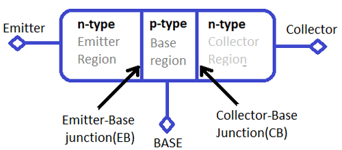
Transistor consists of three layers of semiconductor, which have an ability to hold current. The electricity conducting material such as silicon and germanium has the ability to carry electricity between conductors and insulator which was enclosed by plastic wires. Semiconducting materials are treated by some chemical procedure called doping of the semiconductor. If silicon is doped with arsenic, phosphorous & antimony, it will obtain some extra charge carriers i.e., electrons, are known as N-type or negative semiconductor whereas if silicon is doped with another impurities like as boron, gallium, aluminum, it will obtain fewer charge carriers i.e., holes, are known as a P-type or positive semiconductor.
How Does Transistor Work?
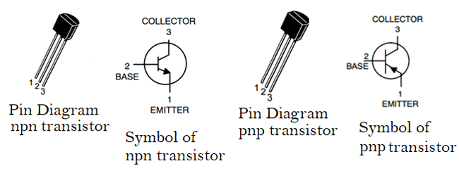
The working concept is the main part to understand how to use a transistor or how it works?, there are three terminals in the transistor:
• Base: It gives base to the transistor electrodes.
• Emitter: Charge carriers emitted by this.
• Collector: Charge carriers collected by this.
If the transistor is NPN type, we need to apply a voltage of 0.7v to trigger it and as the voltage applied to base pin the transistor turns ON which is the forward biased condition and current start flowing through the collector to emitter (also called saturation region). When the transistor is in reversed biased condition or the base pin is grounded or having no voltage on it the transistor remain in OFF condition and not allow the current flow from collector to emitter(also called cut-off region).

If the transistor is PNP type, it’s normally in ON state but not to be said perfectly on till the base pin gets perfectly grounded. After grounding base pin the transistor will be in reverse biased condition or said to be turned ON. As the supply provided to the base pin it stops conducting current from collector to emitter and the transistor said to be in OFF state or forward biased condition.

For the protection of the transistor we connect a resistance in series with it, for finding the value of that resistance we use the formula below:
RB = VBE / IB
Different Types of Transistors:
Mainly we can divide the Transistor in two categories Bipolar Junction Transistor (BJT) and Field Effect Transistor (FET). Further we can divide it like below:

Bipolar Junction Transistor (BJT)
A Bipolar junction transistor is made up of doped semiconductor with three terminals i.e., base, emitter & collector. In this procedure, holes and electrons both are involved. A large amount of current passing into collector to emitter switches up by modifying small current from base to emitter terminals. These are also called as current controlled devices. NPN and PNP are two prime parts of BJTs as we discussed earlier. BJT turned on by giving input to base because it has lowest impedance for all transistors. Amplification is also highest for all transistors.
The types of BJT are as follows:
1. NPN Transistor:
In the NPN transistor middle region i.e., base is of p-type and the two outer regions i.e., emitter and collector are of n-type.

In forward active mode, the NPN transistor is biased. By dc source Vbb, the base to emitter junction will be forward biased. Therefore, at this junction depletion region will be reduced. The collector to base junction is reverse biased, collector to base junction depletion region will be increased. The majority charge carriers are electrons for n-type emitter. The base emitter junction is forward biased so electrons move towards base region. Therefore, this causes the emitter current Ie. The base region is thin and lightly doped by holes, electron–holes combination formed and some electrons remain in base region. This causes very small base current Ib. The base collector junction is reversed biased to holes in the base region and electrons in the collector region but it is forward biased to electrons in base region. Remaining electrons of base region attracted by collector terminal cause collector current Ic. Check more about NPN Transistor here.

2. PNP Transistor:
In the PNP transistor middle region i.e., base is of n-type and the two outer regions i.e., collector and emitter are of p-type.

As we discussed above in NPN transistor, it is also operating in active mode. The majority charge carriers are holes for p-type emitter. For these holes, the base emitter junction will be forward biased and moves towards base region. This causes the emitter current Ie. The base region is thin and lightly doped by electrons, electron–holes combination formed and some holes remain in base region. This causes very small base current Ib. The base collector junction is reversed biased to holes in base region and holes in collector region but it is forward biased to holes in base region. Remaining holes of base region attracted by collector terminal cause collector current Ic. Check more about PNP transistor here.

What are Transistor Configurations?
Generally, there are three types of configurations and their descriptions with respect to gain is as follows:
Common Base (CB) Configuration: It has no current gain but has voltage gain.
Common Collector (CC) Configuration: It has current gain but no voltage gain.
Common Emitter (CE) Configuration: It has current gain and voltage gain both.
Transistor Common Base (CB) Configuration:
In this circuit, base is placed common to both input and output. It has low input impedance (50-500 ohms). It has high output impedance (1-10 mega ohms).Voltages measured with respect to base terminals. So, input voltage and current will be Vbe & Ie and output voltage and current will be Vcb & Ic.
- Current Gain will be less than unity i.e., alpha(dc)= Ic/Ie
- Voltage gain will be high.
- Power gain will be average.

Transistor Common Emitter (CE) Configuration:
In this circuit, the emitter is placed common to both input and output. The input signal is applied between base and emitter and the output signal is applied between collector and emitter. Vbb & Vcc are the voltages. It has high input impedance i.e., (500-5000 ohms). It has low output impedance i.e., (50-500 kilo ohms).
- Current Gain will be high(98) i.e., beta(dc) =Ic/Ie
- Power gain is upto 37db.
- Output will be 180 degrees out of phase.

Transistor Common Collector Configuration:
In this circuit, collector is placed common to both input and output. This is also known as emitter follower. It has high input impedance (150-600 kilo ohms).It has low output impedance(100-1000 ohms).
- Current gain will be high(99).
- Voltage gain will be less than unity.
- Power gain will be average.

Field Effect Transistor (FET):

Field Effect Transistor contains the three regions such as a source, a gate, a drain. They are termed as voltage controlled devices as they control the level of voltage. To control the electrical behavior, the externally applied electric field can be chosen that’s why called as field effect transistors. In this, current flows due to majority charge carriers i.e., electrons, hence also known as the uni-polar transistor. It has mainly high input impedance in mega ohms with low frequency conductivity between drain and source controlled by electric field. FETs are highly efficient, vigorous & lesser in cost.
Field effect transistors are of two types i.e., Junction field effect transistors (JFET) and Metal oxide field effect transistors (MOSFET).The current passes between the two channels named as n-channel and p-channel.
Junction Field Effect Transistor (JFET)
The junction field effect transistor has no PN junction but in place of high resistivity semiconductor materials, they form n& p type silicon channels for flow of majority charge carriers with two terminals either drain or a source terminal. In n-channel, flow of current is negative whereas in p-channel flow of current is positive.


Working of JFET:
There are two types of channels in JFET named as: n-channel JFET & p-channel JFET
N-Channel JFET:
Here we have to discuss about principal operation of n-channel JFET for two conditions as follows:
First, When Vgs=0,
Apply small positive voltage to drain terminal where Vds is positive. Due to this applied voltage Vds, electrons flow from source to drain cause drain current Id. Channel between drain and source acts as resistance. Let n-channel be uniform. Different voltage levels set up by drain current Id and moves from source to drain. Voltages are highest at drain terminal and lowest at source terminal. Drain is reverse biased so depletion layer wider here.
Vds increases, Vgs=0 V
Depletion layer increases, channel width reduces. Vds increases at level where two depletion region touch, this condition known as pinch –off process & causes pinch off voltage Vp.
Here, Id pinched –off drops to 0 MA & Id reaches at saturation level. Id with Vgs=0 known as drain source saturation current (Idss). Vds increased at Vp where current Id remains same & JFET acts as a constant current source.
Second, When Vgs does not equal to 0,
Apply negative Vgs and Vds varies. The width of depletion region increases, channel becomes narrow and resistance increases. Lesser drain current flows & reaches upto saturation level. Due to negative Vgs, saturation level decreases, Id decreases. Pinch –off voltage continuously drops. Therefore it is called voltage controlled device.

Characteristics of JFET:
The characteristics shown different regions which are as follows:
Ohmic Region: Vgs=0, depletion layer small.
Cut-Off Region: Also known as pinch off region, as channel resistance is maximum.
Saturation or Active Region: Controlled by gate source voltage where drain source voltage is lesser.
Breakdown Region: Voltage between drain and source is high cause breakdown in resistive channel.

P-Channel JFET:
p-channel JFET operates same as n-channel JFET but some exceptions occurred i.e., Due to holes, channel current is positive &Biasing voltage polarity needs to be reversed.
Drain current in active region:
Id= Idss[1-Vgs/Vp]
Drain source channel resistance: Rds= delta Vds/delta Id

Metal Oxide Field Effect Transistor (MOSFET):
Metal Oxide Field Effect Transistor is also known as voltage controlled field effect transistor. Here, metal oxide gate electrons insulated electrically from n-channel & p-channel by thin layer of silicon dioxide termed as glass.
The current between drain and source is directly proportional to input voltage.
It is a three terminal device i.e., gate, drain & source. There are two types of MOSFET by functioning of channels i.e., p-channel MOSFET & n-channel MOSFET.
There are two forms of metal oxide field effect transistor i.e., Depletion Type & Enhancement Type.
Depletion Type: It requires Vgs i.e., gate-source voltage to switch off & depletion mode is equal to normally closed switch.
Vgs=0, If Vgs is positive, electrons are more & if Vgs is negative, electrons are less.

Enhancement Type: It requires Vgs i.e., gate source voltage to switch on & enhancement mode is equal to normally open switch.
Here, the additional terminal is substrate used in grounding.

Gate source voltage (Vgs) is greater than the Threshold voltage (Vth)

Modes of Biasing For Transistors:
Biasing can be done by the two methods i.e., forward biasing and reverse biasing whereas depending on biasing, there are four different circuits of biasing as follows:
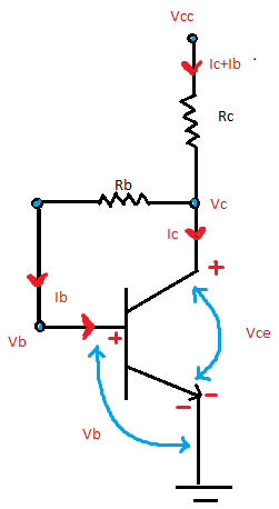
Fixed Base Bias and Fixed Resistance Bias:
In the figure, the base resistor Rb connected between the base and the Vcc. The base emitter junction is forward biased due to voltage drop Rb which leads to flow Ib through it. Here Ib is obtained from:
Ib=(Vcc-Vbe)/Rb
This results in stability factor (beta +1) which leads to low thermal stability. Here the expressions of voltages and currents i.e.,
Vb=Vbe=Vcc-IbRb
Vc=Vcc-IcRc=Vcc-Vce

Ic = Beta Ib
Ie=Ic

Collector Feedback Bias:
In this figure, the base resistor Rb connected across collector and base terminal of transistor. Therefore base voltage Vb and collector voltage Vc are similar to each other by this
Vb =Vc-IbRb

Where,
Vb=Vcc-(Ib+Ic)Rc
By these equations, Ic decreases Vc, which reduces Ib, automatically Ic reducing.
Here, (beta +1) factor will be less than one and the Ib leads to reduce amplifier gain.
So, voltages and currents can be given as-
Vb=Vbe
Ic= beta Ib

Ie is almost equals to Ib
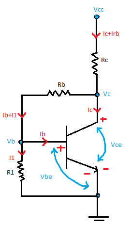
Dual Feedback Bias:
In this figure, it is the modified form over the collector feedback basing circuit. As it has additional circuit R1 which increases stability. Therefore, increase in base resistance leads to the variations in beta i.e., gain.
Now,
I1=0.1 Ic
Vc= Vcc-(Ic+I(Rb)Rc
Vb=Vbe=I1R1=Vc-(I1+Ib)Rb

Ic= beta Ib

Ie is almost equals to Ic
Fixed Bias With Emitter Resistor:
In this figure, it is same as fixed bias circuit but it has an additional emitter resistor Re connected. Ic increases due to temperature, Ie also increases which again increases the voltage drop across Re. This results in reduction in Vc, reduces Ib which brings iC back to its normal value. Voltage gain reduces by presence of Re.
Now,
Ve=Ie Re
Vc=Vcc – Ic Rc
Vb=Vbe+Ve
Ic= beta Ib

Ie is almost equals to Ic

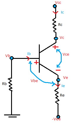
Emitter Bias:
In this figure, there are two supply voltages Vcc & Vee are equal but opposite in polarity.Here,Vee is forward biased to base emitter junction by Re & Vcc is reverse biased to collector base junction.
Now,
Ve= -Vee+Ie Re
Vc= Vcc- Ic Rc
Vb=Vbe+Ve
Ic= beta Ib

Ie is almost equal to Ib

Where, Re>>Rb/beta

Vee>>Vbe
Which gives a stable operating point.
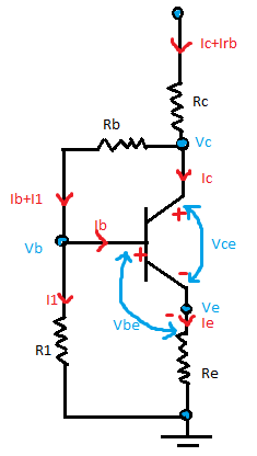
Emitter Feedback Bias:
In this figure, it uses both collector as feedback & emitter feedback for higher stability. Due to flow of emitter current Ie, the voltage drop occur across emitter resistor Re, therefore the emitter base junction will be forward bias. Here, the temperature increases, Ic increases, Ie also increases. This leads to a voltage drop at Re, collector voltage Vc decreases & Ib also decreases. This results that the output gain will be reduced. The expressions can be given as:
Irb=0.1 Ic=Ib+I1
Ve=IeRe=0.1Vcc
Vc=Vcc-(Ic+Irb)Rc
Vb=Vbe+Ve=I1R1=Vc-(I1+Ib0Rb)
Ic=beta Ib

Ie is almost equal to Ic
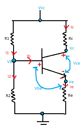
Voltage Divider Bias:
In this figure, it uses voltage divider form of resistor R1 & R2 to bias the transistor. The voltage forms at R2 will be base voltage as it forward biases the base-emitter junction. Here, I2= 10Ib.
This is done to neglect voltage divider current and changes occur in value of beta.
Ib=Vcc R2/R1+R2

Ve=Ie Re

Vb=I2 R2=Vbe+Ve
Ic resist the changes in both beta & Vbe which results in a stability factor of 1.In this, Ic increases by increase in temperature, Ie increases by increase in emitter voltage Ve which reduces the base voltage Vbe. This results in decrease base current ib and ic to its actual values.
Applications of Transistors
- Transistors for the most of the parts are used in electronic application such as voltage and power amplifiers.
- Used as switches in many circuits.
- Used in making digital logic circuits i.e., AND, NOT etc.
- Transistors are inserted in everything i.e., stove tops to the computers.
- Used in the microprocessor as chips in which billions of transistors are integrated inside it.
- In earlier days, they are used in radios, telephone equipment’s, hearing head’s etc.
- Also, they are used earlier in vacuum tubes in big sizes.
- They are used in microphones to change sound signals into electrical signals as well.

I'm teacher, I liked that.