
EasyEDA is a Cloud based free online service to design Circuit Schematics, simulate circuits, convert schematics into PCB Layout and manufacture PCBs for end users and industries. This all can be done at one place with EasyEDA online tool. We have already covered this tool in detail in this article EasyEDA for Electronic Circuit Design and demonstrated whole process, with an example, from drawing circuit to order PCB here.
Now EasyEDA has launched a new tool that is Online Gerber Viewer. Gerber file is generated by PCB CAD tool and basically used to fabricate the PCBs, it is an open ASCII vector format for 2D binary images, used to describe the PCBs images: copper layers, solder mask, legend, etc. Generally any PCB manufacture would ask for Gerber file to fabricate that PCB. So we can view these Gerber files using the EasyEDA Gerber viewer.
EasyEDA’s online Gerber viewer supports the standard RS-274X format and takes Gerber files in zipped format, and then generates the images of Top and Bottom layer of PCB. At the same time, EasyEDA runs a simple Design For Manufacture (DFM) check, from which you can see the board size, hole and track sizes and clearances of the various PCB objects such as tracks and pads. So you can see images and check all the detail of PCB before ordering them.
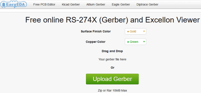
If you have Gerber Files for your PCB, then you can directly go to https://gerber-viewer.easyeda.com/ and upload the files there to view them as images. See below images:
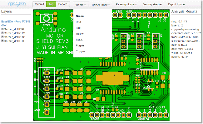
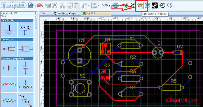
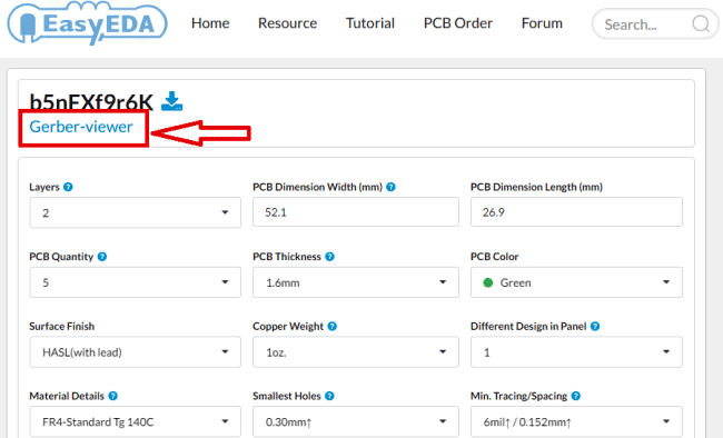
If you create schematic and PCB layout using EasyEDA then its very easy to see them in Gerber Viewer. You just need to click on ‘Fabrication Output’ button in PCB Schematic Screen, it takes you to the ‘Order page’, where you will find the Link to view your PCB layout in Gerber viewer. Click on this link and you can see your PCB as a detailed Gerber View. See the images below:
In Gerber Viewer you can find lot of options and settings, like:
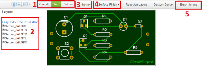
1. You can see the Top and/or Bottom layer of PCB.
2. You can enable and disable various Gerber files to see the effects on PCB image, like *.GTO file contains the silk top layer, so you can see it separately.
3. You have ‘theme’ option to select the PCB in different colors.
4. You have ‘Surface Finish’ option to see the Pads and junctions in Gold or Silver colors.
5. You can also Export any view or layer or any Gerber file as Image file using the Export button.
There are lot more cool options, just upload your Gerber file and check them out.
So with this launching of new Gerber viewer tool, EasyEDA becomes the one stop solution from drawing the circuits to taking down them on PCB for professional and industrial use.
