
EasyEDA is a free EDA tool for individuals and working in a web browser, it requires no any installation. It was designed to provide electronic hobbyists, engineers, teachers, students ... an easy and free access to the EDA. With EasyEDA, powerful schematic capture, mixed-mode spice simulation and PCB layout are made in your web browser. EasyEDA has all the features you expect and easily take your design from conception through to production. EasyEDA aims to bring every electronic hobbyist an easier EDA experience. That’s why EasyEDA comes to the world and named EasyEDA.
EasyEDA Features
Here is how EasyEDA introduces its online PCB creation tool. The main features of the tool are as follows:
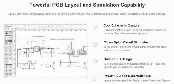
Draw diagrams quickly in your browser using the available libraries. The updates will be applied automatically.
Check analog, digital and mixed circuits with sub-circuits and SPICE models!
With multiple layers, thousands of blocks, you can always work quickly and smoothly arrange your cards.
Design Flow using EasyEDA
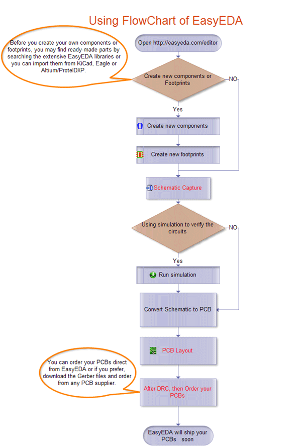
Steps applied to the creation of a blinking LED with 555 IC
Google Chrome application
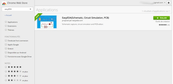
EasyEDA is available in the Chrome store.
Once the app is installed if you display the apps (type in the address bar of Chrome: chrome: // apps)
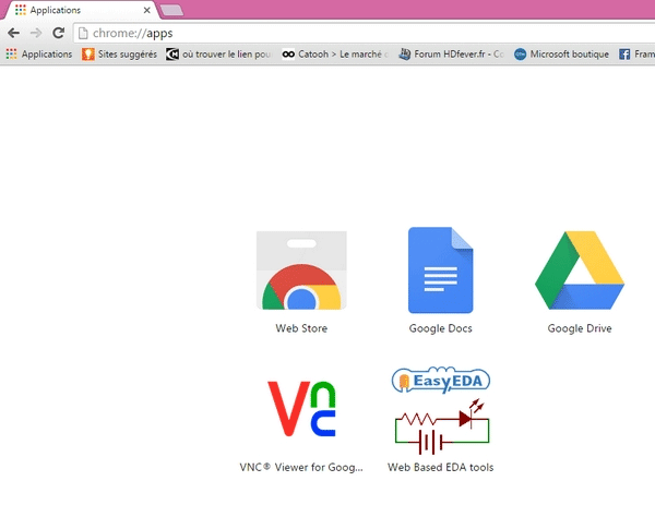
and you click on the app EasyEDA, then you arrive on the EasyEDA website:
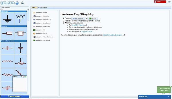
On the left side of the screen, you find symbols that you select when you click on it. On the right side you can choose to draw a schematic or directly a PCB (printed circuit board).
Draw which circuit ?
For a former electronics engineer like me, it was easy to find a simple circuit for testing the use of this web app. How about a good old 555 IC? I largely use it during my career, I will use it this time again.
And as output I use a LED to « see » what happen…
Drawing the schematic
The interface already seen a little higher is very simple to use. Select a component in the left column by clicking it. Move the mouse in the drawing window. Click, you release the component. Click again, you release another one... The space bar and the R key are used to rotate the components. The numbers increment automatically. Here is the diagram that I realized.
Circuit simulation
 if you look at the schematic, you'll see I've added two probes volProbe1 and volProbe2. It is possible to start the simulation by clicking on the icon representing a jogger then Run the Document.
You will have to set the parameters in order to observe the curves generated by the simulator. After a few tries, the simulation result appears.
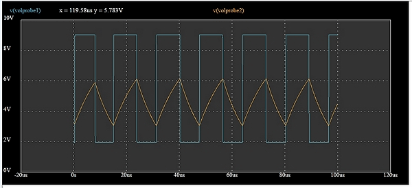
We can see the charge / discharge of the capacitor and the output voltage. To better see the results I enlarged the image by adjusting the time (µs/div).
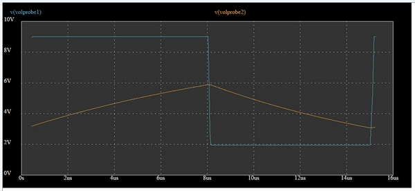
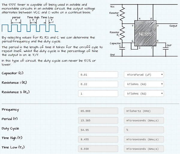
If you look at the 555 calculator a little higher, you will see that the period should be worth 15.385 microseconds ... not bad, right?
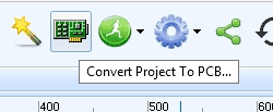 Once verified the proper operation of the circuit, click on the printed circuit card icon and you start the creation of the PCB.
The first step is the generation of the net where the components are connected by direct wires.
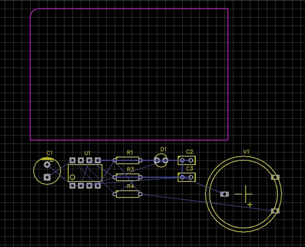
From this net, move the components on the board according to your placement constraints (here I did not have any )
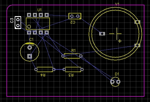
 Well ... we begin to see what will look like the circuit ... You can now route the tracks.
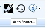
You click on the icon representing printed circuit tracks and go!. The first window asks you information on the size of the tracks. You can also avoid routing some tracks as the ground for example, if you are planning to use ground plane ... At first simply confirm by clicking on RUN.
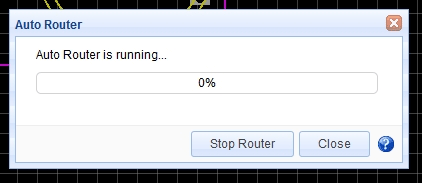
With the 555 diagram, routing takes only a few seconds ... it certainly will not be the case with a more complex schematic.
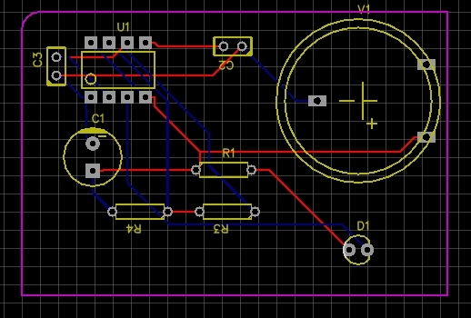
The color of tracks indicates whether they are above or below the circuit.
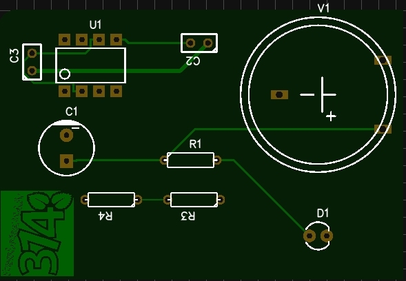
We can add tracks, change the width, move some tracks by clicking on the active points, for example I shifted the blue one that passes under R4 and that seemed too close to the pad. I also do a U-turn to LED D1 (bottom right) because the tracks crossed. In this case you must restart the routing and lose your changes to the tracks width. It is therefore necessary to redo tracks width modification. Please ensure that all components are correctly positioned before changing tracks width !
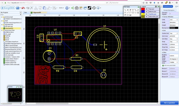
You can insert an image, a logo on the PCB :
![]()
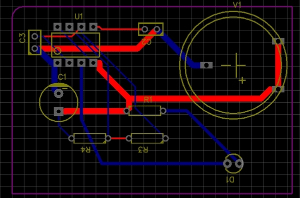
The different layers of the board are displayed using a color code. Here the yellow color indicates that we visualize the top silk layer printed on the top of the circuit.
We can finally see a photographic view of the circuit to have an idea of what it will look like.
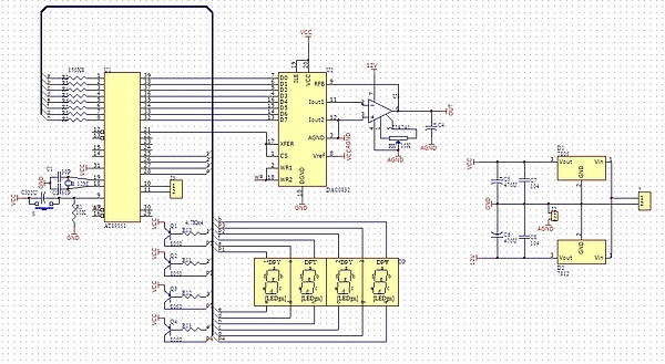
More advanced examples
Well, okay, my basic 555 circuit is not very representative ... It allowed me to test the workflow and verify the operation of this free tool.
Of course with a little more time (and a lot more experience) you can produce circuits quite professional, examples of which are available on the website:
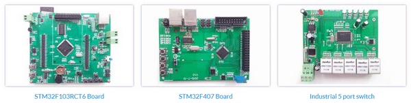
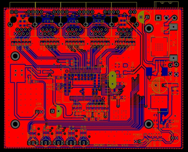
4 ports Switch
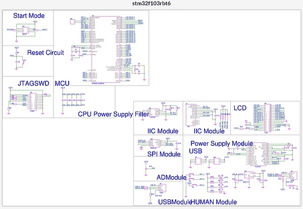
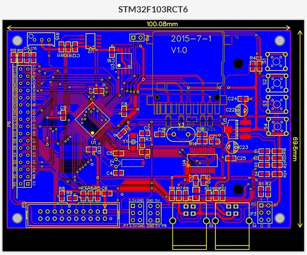
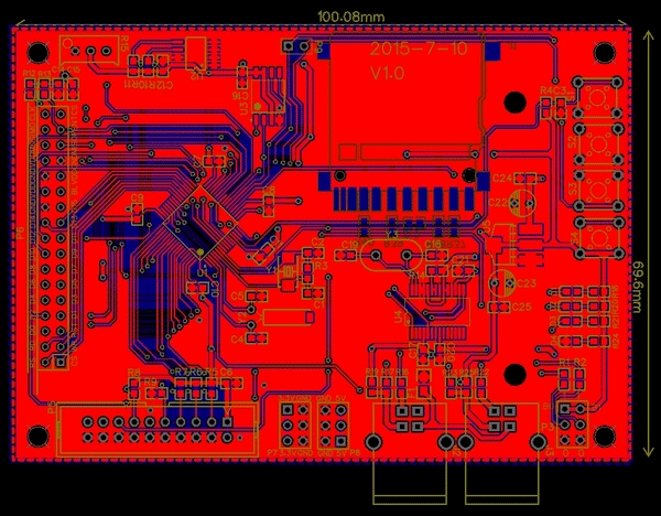
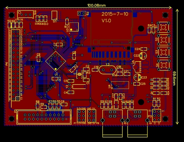
STM32 board :
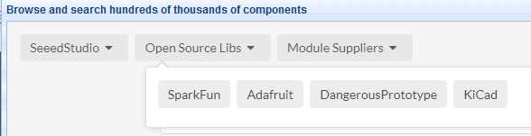
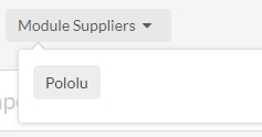
Use open source modules
EasyEDA also provides component libraries that allow you to directly integrate components from multiple vendors :
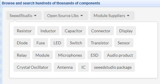
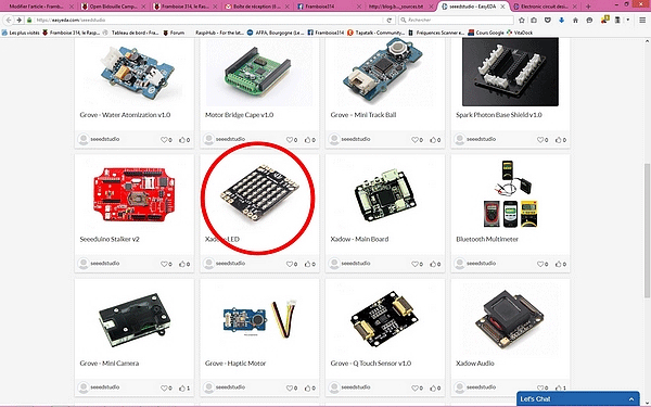
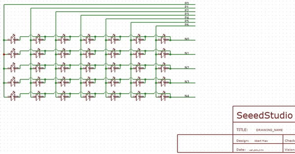
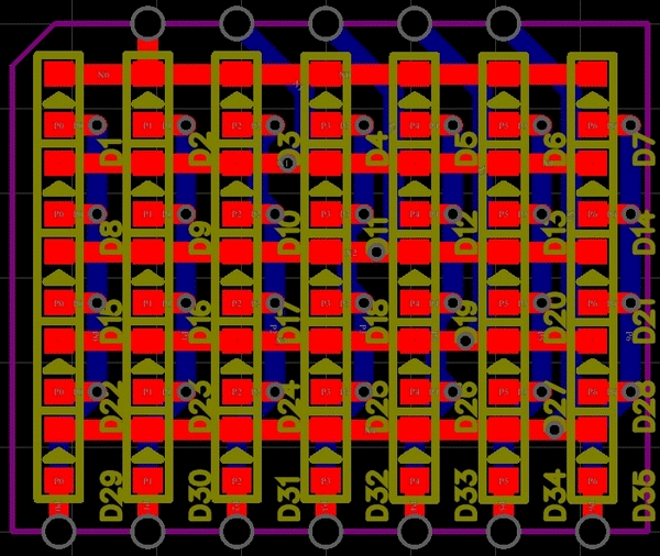
To illustrate this I have chosen an LED equipped module (SeeedStudio). It is possible to integrate this module to your project :
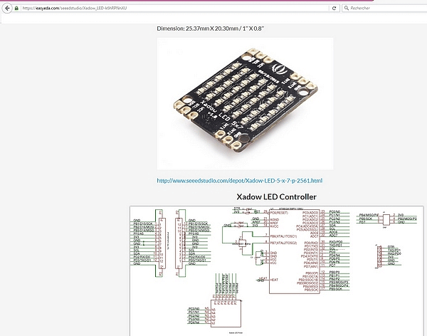
EasyEDA has a rich library of thousands of electronic components (for schematics, PCB and modeling) and tens of thousands of examples of schematics! Anyone can use this library and enrich it. You can also import drawings made in Altium, Eagle and KiCad and edit in EasyEDA.
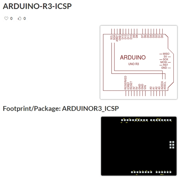
It includes the Arduino in all forms such as R3:
Create the PCB
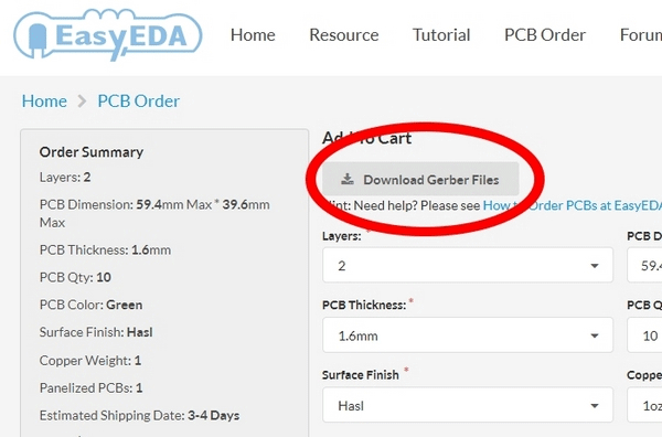
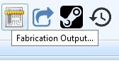 When you are satisfied with your circuit, Fabrication Output icon directs you to the page where you can choose to download the Gerber files (if you want them manufactured by another manufacturer) or continue by ordering the printed circuit to EasyEDA.
Tutorial on How to Use EasyEDA
A comprehensive tutorial describes how to use EasyEDA. An online ebook describes how to use the simulator.
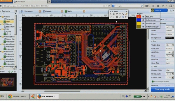
The tutorial is completed with videos that explain the operations, such as the diagram creation :
One can also create professional schematics:
Video
Conclusion
During my tests, which lasted several hours, EasyEDA proved stable, reliable and relatively easy to learn as it is pretty intuitive. One regret though, is that when you have routed and then retouched widths tracks, it requires to restart the routing ... and to redo the track widths modifications. No matter if it was a small circuit like mine. A little annoying if you have a complex drawing !
The availability of a large number of open source modules is more significant, as well as access to thousands of shared projects such as clocks or speed controllers ...
The availability of a tutorial and an ebook for the simulator facilitate the handling of this online app.
Completely free for electronics engineers, educators, students, makers and enthusiasts. Why not try this free and powerful circuit design software. You will find it is interesting and unique.

Great Job
Need help on How to export pcb /schematics gerber file generated from easyEDA To Arduino CNC writer machine made from DVD motors instead of following the process of using photo paper, I want to do direct printing on pcb. N.B.:am a novice but fall in love electronics/program electronics like Arduino.
May circuit digest grow to become worldwide consult home.
Love your great service here.
Thanks a lot